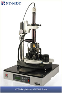
NTEGRA Prima is a multifunctional device for performing the most typical tasks in the field of Scanning Probe Microscopy.
The device is capable of performing more than 40 measuring methods, what allows analyzing physical and chemical properties of the surface with high precision and resolution. It is possible to carry out experiments in air, as well as in liquids and in controlled environment. The new generation electronics provides operations in high-frequency (up to 5MHz) modes. This feature appears to be principal for the work with high-frequency AFM modes and using high-frequency cantilevers.
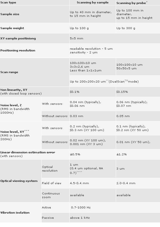
There are several scanning types implemented in NTEGRA Prima: scanning by the sample, scanning by the probe and dual-scanning. On account of that, the system is ideal for investigating small samples with ultra-high resolution (atomic-molecular level) as well as for big samples and scanning range up to 100x100x10 µm. The unique DualScan TM mode allows investigating even bigger fields on the surface (200x200 µm for X, Y and 22 µm for Z) that can be useful, for example, for living cells and MEMS components.
Built-in three axes closed loop control sensors trace the real displacement of the scanner and compensate unavoidable imperfections of piezoceramics as non-linearity, creep and hysteresis. The sensors, which are used by NT-MDT, have the lowest noise level, thus allowing working with closed loop control on the very small fields (down to 10x10 nm). This is especially valuable for carrying out nanomanipulation and lithography modes.
Ntegra Prima has a built-in optical system with 1 µm resolution, which allows imaging the scanning process in real-time.
Due to the open architecture, the functionality of NTEGRA Prima can be extended essentially: specialized magnetic measurements with external magnetic field, high-temperature experiments, Near-field optical microscopy, Raman spectroscopy, etc.
| Scanning Probe Microscopy |
In air&liquid : AFM (contact + semi-contact + non-contact) / Lateral Force Microscopy / Phase Imaging/ Force Modulation/ Adhesion Force Imaging/ Lithography: AFM (Force)
In air only : STM/ Magnetic Force Microscopy/ Electrostatic Force Microscopy/ Scanning Capacitance Microscopy/ Kelvin Probe Microscopy/ Spreading Resistance Imaging/ Lithography: AFM (Current), STM/ AFAM (optional) |
Specifications :

* Scanning head can be configured to serve as a stand-alone device for specimens of unlimited sizes.
** Optionally can be expanded to 200x200x20 ?m.
*** Built-in capacitive sensors have extremely low noise and any area down to 50x50 nm can be scanned with closed-loop control.
**** High Resolution Viewing system (HRV head) is optional and provides additional functionality making it possible to generate and detect tip-localized aperture less near-field effects.
Measuring modes
-
In ambient air:
STM/ STS/ AFM (contact + noncontac + semicontact)/ LFM/ Phase Imaging/ Force Modulation mode/ Spreading Resistance Imaging/ MFM/ EFM/ SCM/ Kelvin mode/ Adhesion Force Imaging/ AFAM/ AFM Lithographies: Force (scratching + dynamic plowing), Current (Local Anodic Oxidation), STM
- In liquid:
AFM (contact + semicontact)/ LFM/ Phase Imaging/ Force Modulation mode/ Adhesion Force Imaging/ AFM Lithography
Applications
-
Biology and Biotechnology
Proteins, DNA, viruses, bacteriums, tissues
-
Materials Science
Surface morphology, surface morphology, local piezoelectric properties, local adhesion properties, local tribological properties
-
Magnetic materials
Magnetic domain structure visualization, observation of magnetization reversal processes that depend on external magnetic field, observation of magnetization reversal processes under different temperatures
-
Semiconductors, electric measurements
Wafers and other structures morphology, local surface potential and capacitance measurements, electric domain structure imaging, determination of heterojunction bounds and semiconductor regions with different doping levels, failure analysis (localization of conductor line failure and leakage in dielectric layers)
-
Polymers and Thin Organic Films
Spherulites and dendrites, polymer monocrystals, polymer nanoparticles, LB-films, thin organic films
-
Data storage devices and medias
CD, DVD disks, storages for terabit memories with thermomechanical, electric and other types of recording
-
Nanomaterials
Nanopowders, nanocomposites, nanoporous materials
-
Nanostructures
Fullerenes, nanotubes, nanofilaments, nanocapsules
-
Nanoelectronics
Quantum dots, nanowires, quantum structures
-
Nanomachining
AFM lithography: force (ac and dc), current (Local anodic oxidation), STM lithography
-
Nanomanipulations
Contact force
|
|


![]()

